


Every day, we use mobile phones, computers, and tablets. We might also drive new energy vehicles and check smartwatches. But have you ever wondered where the most core and mysterious "chips" in these devices come from? Don’t worry. Today, we’ll use the simplest words to take you from a round "cake" to the small chips that power the world.
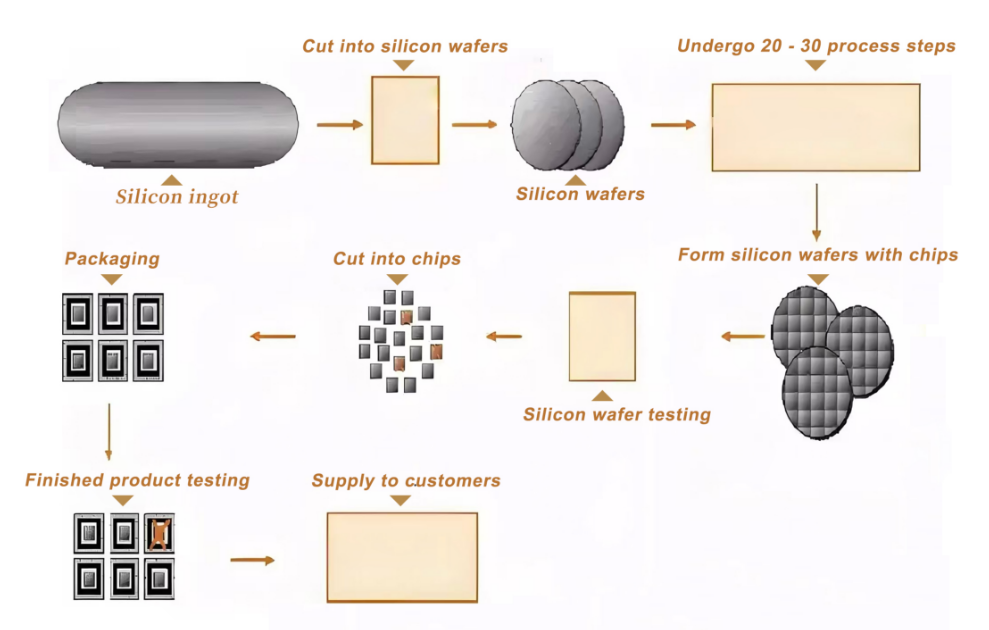
You can think of a wafer as a "big cake made of silicon"—it’s usually a grayish-white round sheet. This "cake" isn’t ordinary silicon stone. It’s highly purified monocrystalline silicon with almost no impurities, and its purity can reach over 99.9999%.
Why is it made round? It’s simple: round shapes are easier to rotate and process during production, and they have a high utilization rate when being cut.
The size of a wafer is measured by its diameter. In the early days, wafers were only 1 or 2 inches (about the size of a ping-pong ball). Later, they became 6 inches and 8 inches. Now, the mainstream size is 12 inches (as big as a pizza). The larger the wafer, the more chips can be cut from it—which means lower costs and higher efficiency.
Are all wafers the same? Of course not! Wafers also have their "report cards":
Prime Wafer (top student): Its surface has almost no defects and its structure is perfect. It’s specially used to make high-performance chips, such as mobile phone processors and GPUs.
Test Wafer (for exam papers): It has a few defects but doesn’t affect its overall use. It’s used for testing or making secondary products.
Monitor Wafer (for monitoring): Its surface has some problems, but its electrical performance is still good. It’s mainly used to monitor the production process.
Rejected Wafer (failed): It has too many defects and can barely be used to make chips.
To put it simply, a wafer is the "big base" for making chips.
Having a wafer doesn’t mean we can use it directly. The wafer goes through complex process steps: lithography, etching, deposition, ion implantation... It’s like carving countless precise circuit patterns on a big cake. Finally, the whole wafer is cut into small pieces—these are called dies.
You can imagine: each triangular slice on a pizza is like a die. But in chip factories, the cuts aren’t triangular—they’re neat squares or rectangles.
Each die is an independent small circuit unit. For example, a single wafer may have hundreds to thousands of dies. Some of these dies are perfect, while others may have small flaws. That’s when testing comes in: we check which dies meet performance standards and which don’t. The ones that pass the test are called "Known Good Dies (KGD)".
Why is there the concept of "bare dies"? Because modern chip packaging methods are getting more and more complex. Sometimes, a chip has more than one "core"—it may need to stack logic chips, memory chips, and radio frequency modules together. This requires combining qualified bare dies like building blocks to form a more powerful system.
So, a die is a "semi-finished chip". It determines whether the final chip can run fast and stably.
The final step is to take these selected good dies and package them. What does packaging do? You can think of it as putting a "protective armor" on the fragile die and adding small "hands and feet" to it, so it can connect with the outside world. Without packaging, a die is as brittle as glass and can’t be used at all.
After packaging and final testing, these small squares become the chips we’re familiar with (also called integrated circuits, or ICs).
How many transistors can fit in one chip? This is simply a miracle of human wisdom. The earliest chips could only hold 5 or 6 transistors. Today, a mobile phone processor can hold billions or even hundreds of billions of transistors!
Why can your mobile phone take photos, play games, scroll through short videos, and run AI? It’s all thanks to this small chip doing rapid calculations. It’s the "brain" of the device and the engine of the entire digital age.
If we use making a cake as an analogy:
Wafer = a whole piece of cake base (round, not cut yet)
Die = small pieces of cake after cutting (each piece may be a little different)
Chip = small cakes that are beautifully packaged, labeled, and sent to consumers
UF Capacitors is an ISO9001-certified manufacturer in China, founded in 1995. We hold military qualifications for tantalum capacitors, MLCC, and other products. Additionally, we have a UL-recognized test laboratory located at our factory site.
Our marketing position is to provide a superior alternative to first-tier brands such as TDK, Murata, AVX, EPCOS, Vishay, and Panasonic. We offer similar quality but at better prices, with faster lead times and excellent service. With extensive experience working with renowned international companies like GE, Philips, Jabil, and Flex, we have built a strong reputation.
UF Capacitors serves the consumer electronics, computing, communications, and industrial markets. As a professional Chinese electronic components manufacturer, we are dedicated to delivering high-quality electronic components, exceptional management, strict quality control systems, and excellent sales service. We strive to foster mutually beneficial partnerships and drive business growth.